


Table of Contents
Buy/Sell Your Unlisted Shares
Submit the details below to share a quote.
India’s semiconductor sector marked an important moment in December 2025 with the announcement of a new high-power UV LED platform by Polymatech Electronics. Unveiled from Chennai, the technology is designed to significantly improve industrial curing processes while reducing energy consumption and environmental impact.
The platform targets industries that rely on rapid and reliable curing of UV-sensitive materials. The system achieves curing times of less than one second, a performance level comparable to conventional mercury vapour lamps. At the same time, it cuts energy usage by as much as 80% which offers manufacturers a more efficient and sustainable alternative.
Technology designed for speed and precision
The new UV LED platform delivers exceptionally high photon flux density, which enables fast and uniform curing of inks, coatings, adhesives, resins and solder masks. One of its key advantages is precise wavelength control in the UVA range of 395 to 405 nanometres. This allows manufacturers to tailor curing performance to specific material chemistries, improving quality and consistency across production lines.
Thermal management has been a major focus in the platform’s design. The system is capable of sustaining continuous output levels above 150 W per square centimetre, even in demanding industrial environments. Its chip-on-board architecture supports long operating life, exceeding 50,000 hours, which helps reduce downtime and maintenance costs.
A safer and more sustainable alternative
Unlike traditional mercury-based curing systems, the UV LED platform operates without mercury, ozone or UVC emissions. This makes it safer for workers and easier for companies to meet environmental and regulatory standards. The move away from mercury lamps also addresses growing global pressure to phase out hazardous substances from industrial processes.
Strengthening India’s position in global semiconductors
With this launch, Polymatech places India among a small group of countries capable of producing advanced UVA and deep-UV LED technologies. These technologies have historically been dominated by manufacturers in Japan, the United States and Europe. The company plans to present a live demonstration of the platform at CES 2026 in Las Vegas, aiming to attract global original equipment manufacturers and industrial buyers.
Company leadership has described the development as a major step forward for India’s semiconductor ecosystem. The project aligns with the broader Atmanirbhar Bharat vision, which focuses on building domestic capabilities in critical technologies.
Wide-ranging industrial applications
The UV LED platform is designed for use across a broad range of sectors. These include resin-based 3D printing and additive manufacturing, electronics production such as PCB coatings and solder masks, high-speed industrial and digital printing, automotive refinishing, medical device assembly, along advanced packaging and labelling.
Production and market rollout plans
Pilot production has already begun at Polymatech’s Chennai facility. To meet anticipated global demand, the company is also scaling operations at a new manufacturing site in Singapore. Commercial shipments are scheduled to begin in the first quarter of 2026, indicating a swift transition from development to market deployment.
Overall, the new high-power UV LED platform represents a significant step toward more efficient, cleaner, and faster industrial curing, while also highlighting India’s growing role in advanced semiconductor manufacturing.
You may also like to read

What Are The Different Classes Of Shares Issued In India?

Different Classes of Assets In The Financial Market

Follow These Simple Share Market Tips While Investing

Importance of Investing in Unlisted Shares

Step-by-step Process Of Transferring Unlisted Shares (Off-market)

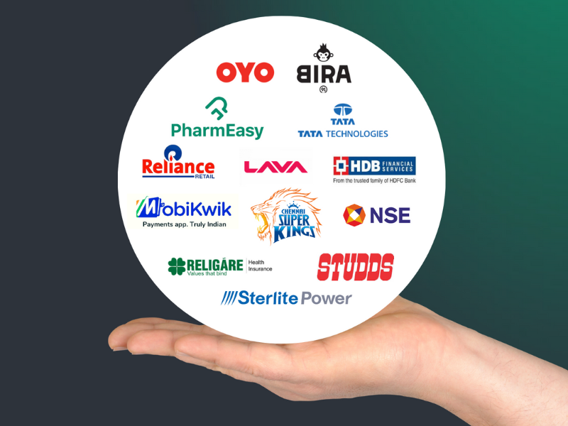
Pre IPO Success Stories To Start Your Unlisted Share Trading

What Is The Expected Return Of Unlisted Shares?

A Detailed Guide On How To Buy Unlisted Shares In India

Know Your Tax Implications Before Investing In Unlisted Shares
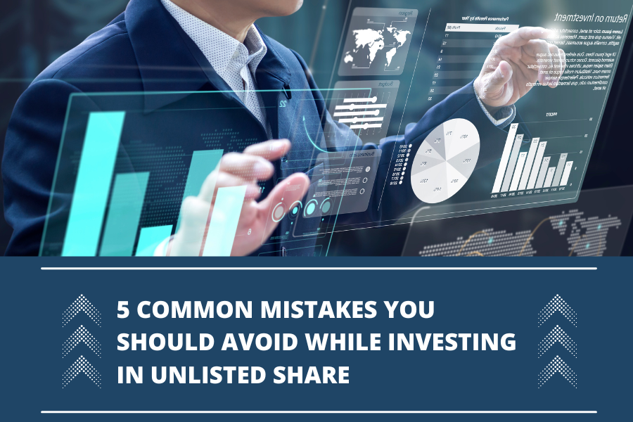
Common Mistakes To Avoid While Investing In Unlisted Shares
How To Pick Best Performing Unlisted Stocks in India?

Risks And Rewards Associated With Unlisted Share Investment
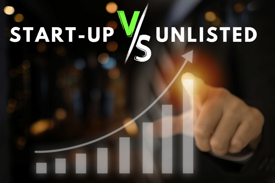
Difference Between Start-Up Investing And Unlisted Shares?

IPO Process in India: Key Steps Explained Clearly

Revealed: The Real Picture of Unlisted Shares in Grey Market

Key Financial Ratios And How To Use Them To Analyse Your Investment

101 Guide For Beginners: What Is Pre IPO Share Market?

10 Golden Rules Of Investing In Stock Market

Listed Shares Vs. Unlisted Shares - Detailed Comparison

The Dark Side of Paytm's IPO Explained In Details

What Leads to Delisting of Shares and What Goes Behind The Scenes?

When Should You Review Your Portfolio Professionally?

In-Depth Analysis of Pre-IPO Shares for Portfolio Growth

PharmEasy Unlisted Price Falls 70%. Here's why

Delaying Pre-IPO Investments? Here’s What You Risk

An NRI’s Guide To Invest In Unlisted Shares In India

Guide To Filter The Most Profitable Unlisted Companies In India

A Comprehensive Guide On Follow-on Stocks

Care Health Insurance

Smart Strategy to Buy & Sell Unlisted Shares Professionally

Top Highly Profitable Unlisted Companies In India To Look For As An Investor

Upcoming IPOs In 2022-2023

Expert’s Driven Roadmap To Research A Startup IPO

Capgemini Unlisted Shares: Is The Risk Worth?

HDFC Sec vs HDB Financial: Which Is the Better Pick?

Detailed Guide To Calculate Capital Gains on Unlisted Shares

Dematerialisation of Unlisted Shares and Its Impact On Shareholders

How are B9 Beverages Pvt Ltd (Bira91) Unlisted Shares Gaining Pace Again?

Reliance Retail: The Success Story of India's Largest Retail Brand

The Future Of Unlisted Shares In the Fintech Market
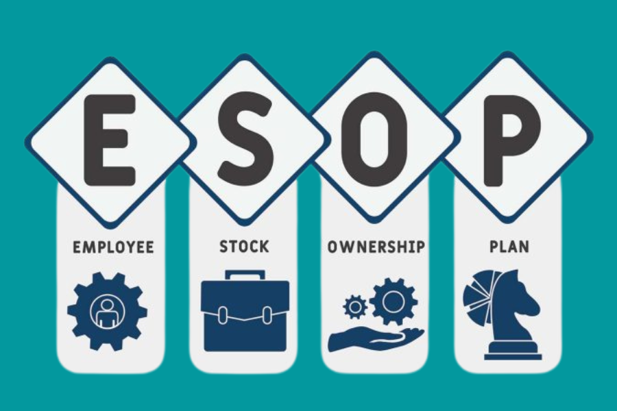
Employee Stock Ownership Plan: What, How, and Why?

Studds Unlisted Shares: 6 Reasons to Buy Now
LAVA’s Unlisted Shares Soar Under Atmanirbhar Push

NSE vs BSE: Detailed 101 Market Share Comparison

The Role Of Corporate Governance And Management In Unlisted Companies
What's Temperature Ahead Of Tata Technologies' ₹4,000 Cr. IPO?

The Future Outlook For Unlisted Shares As An Investment Option

How to Buy and Sell Unlisted Shares in India?

The Benefits And Drawbacks Of Investing In Unlisted Shares